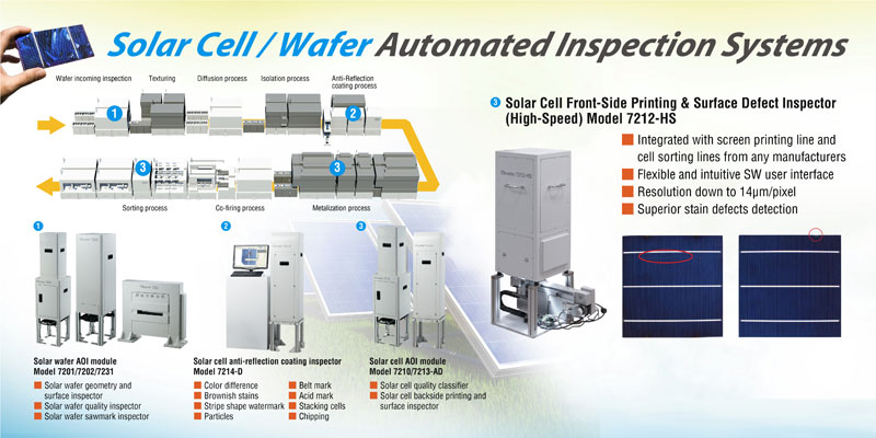
Among several fac tor s for PV to achieve grid-parity, reliability of the PV modules plays an important role. Since it's known that some of the cell defects such as edge chips/ flakes, bumps of cell surface were proved to be source of infant mortality of the c-Si PV modules, therefore, to detect those defects is very important for c-Si cell manufacturers.
However, most of cell defects are inherited by wafers. Therefore, both cell and wafer defect inspections are crucial to final PV module quality and reliability.
Due to the inc rea s ing BIPV and roof top application, even for those defects that does not directly link to reliability issues such as water mark, surface stain, have to detected and considered as fail or secondary grade of cells for c-Si cell buyers.
Conventionally, those defects were visually inspected by operators. But, the inconsistent inspect result makes fully automatic optical inspection (AOI) solution becomes unavoidable equipment for c-Si cell & wafer lines.
Chroma 7200 series are specially designed for detecting wide variety of defects observed for c-Si cells & wafers for all sizes and crystallizations. Base on the process needs, eight inspectors are available for both incoming wafer and final cell sorting requirements.

| Function Guide |
7201 |
7202 |
7210 |
7212-HS |
7231 |
7213-AD |
7214-D |
| Sawmark |
|
|
|
|
✔ |
|
|
Geometry
(Length, angle, area,...etc) |
✔ |
|
|
|
|
|
|
Surface stain
(Particle, water mark, finger print,...etc) |
✔ |
✔ |
✔ |
✔ |
|
✔ |
✔ |
Printing defect
(Fat, interruptions, nodes,...etc) |
|
|
✔ |
✔ |
|
✔ |
|
Color defect
(Coloring, variation, spot,...etc) |
|
|
✔ |
✔ |
|
|
✔ |
| |
More Information |
More Information |
More Information |
More Information |
More Information |
More Information |
More Information |