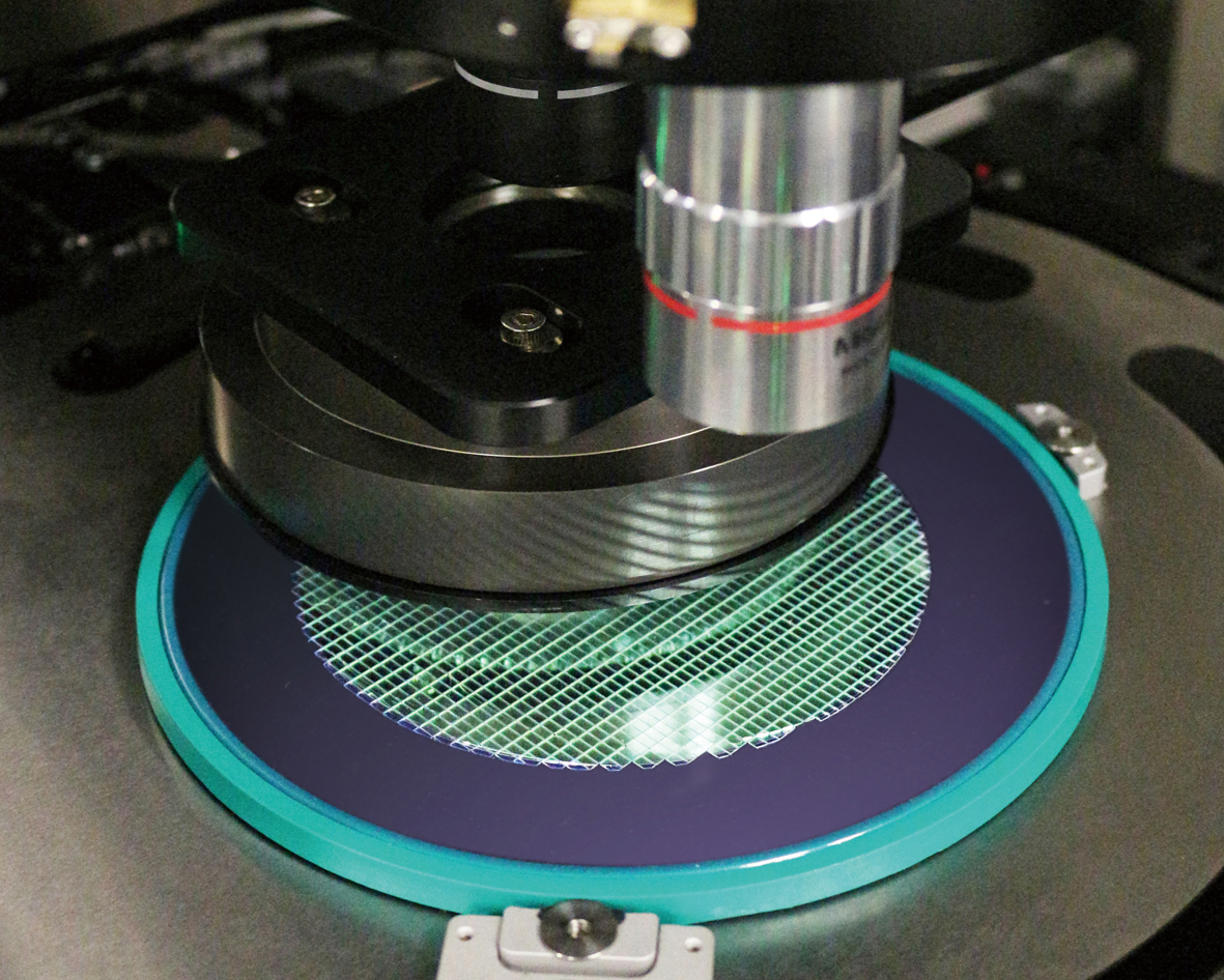
Chroma 7940 wafer chip inspection system is an automated inspection system for postdiced wafer chip inspection. It is capable of inspecting both top and bottom view of the wafer chip simultaneously. Utilizing an advanced illumination technology and color camera acquisition, the system can be customized for various wafer processes and test configuration such as vertical chip or flip chip inspection.
With high-speed camera and inspection algorithms, Chroma 7940 can inspect up to 6" wafer in 3 minutes with a throughput of up to 15 msec./chip. It provides auto focus and compensation for wafer warpage and leveling of an uneven chuck. 2X and 5X magnifications with 1.3μm/pixel and 0.5μm/pixel resolutions respectively are used to detect various defects down to 1.5μm in size.
System Function
After tape expansion, individual chip orientation may become irregular and chip realignment is needed during the inspection process. Chroma 7940 includes a software alignment function that automatically adjusts wafer alignment angle for precision scanning. The system comes with an easy-to-read and user-friendly interface that significantly reduces user's learning time while providing visual wafer mapping of defect regions and inspection result.
Defect Analysis
Besides pass/fail inspection and bin data, all raw data for the inspection result may be recorded for further analysis. This database makes it easy to analyze and obtain optimal parameters for balancing the over-kill and under-kill. It is also used to monitor defect trend caused by the production process, therefore capable of providing advanced feedback for production control.
Applications
| LED Top Side Defects |
- Pad Defect
- Pad Residue
- ITO Peeling
- Finger Broken
- Mesa Abnormality
- Epi Defect
- Chipping
- Chip Residue
|

▲ Front side image with co-axis light
|

▲ Front side image with ring light
|
| LED Back Side Defects |
- Dicing Abnormality
- Pad Bump
- Chipping
- Metal Lack
|

▲ Back side image with co-axis light
|

▲ Back side image with ring light
|
| VCSEL Top Side Defects |
- Pad Defect
- Pad Scratch
- Emitting Area Defect
- Peeling
- Mesa Abnormality
- Epi Defect
- Chipping
- Chip Residue
|

▲ Front side image with co-axis light
|

▲ Front side image with ring light
|
| VCSEL Back Side Defects |
- Dicing Abnormality
- Pad Bump
- Chipping
- Metal Lack
|

▲ Back side image with ring light
|